59 questions0 / 59 done
Questions per paper
- All
- MCQ
- MSQ
- NAT
2015 to 2026. Point at a year to read it.
Show as a table
| Year | All | MCQ | MSQ | NAT |
|---|---|---|---|---|
| 2015 | 0 | 0 | 0 | 0 |
| 2016 | 4 | 4 | 0 | 0 |
| 2017 | 2 | 1.5 | 0 | 0.5 |
| 2018 | 5 | 4 | 0 | 1 |
| 2019 | 7 | 7 | 0 | 0 |
| 2020 | 4 | 3 | 0 | 1 |
| 2021 | 7 | 1 | 0 | 6 |
| 2022 | 7 | 5 | 0 | 2 |
| 2023 | 6 | 2 | 1 | 3 |
| 2024 | 6 | 4 | 0 | 2 |
| 2025 | 5 | 4 | 0 | 1 |
| 2026 | 4 | 3 | 0 | 1 |
- 1EE 2026 · 1 mark · NAT · ModerateIn the linear regulator circuit shown, the base to emitter voltage of the BJT is . The Zener diode clamps the base voltage to . Ignore the biasing current of the Zener diode and BJT.
- 2EE 2026 · 2 marks · MCQ · ModerateIn the circuit shown, the open loop gain of the operational amplifier is .
- 3EE 2026 · 2 marks · MCQ · ModerateThe digital circuit shown has 3 inputs (, , and ).
- 4EE 2026 · 2 marks · MCQ · ModerateThe MOSFET switches shown in the circuit are ideal.
- 5EE 2025 · 1 mark · MCQ · EasyWhich one of the following statements is true about the small signal voltage gain of a MOSFET based single stage amplifier?
- 6EE 2025 · 1 mark · MCQ · ModerateAssuming ideal op-amps, the circuit represents a
- 7EE 2025 · 2 marks · MCQ · ModerateA Boolean function is given as
- 8EE 2025 · 2 marks · MCQ · HardIn the circuit, is an ideal current source. The transistors and are assumed to be biased in saturation, wherein is the input signal and is fixed DC voltage. Both transistors have a small signal resistance of and trans-conductance of . The small signal output impedance of this circuit is
- 9EE 2025 · 2 marks · NAT · ModerateThe op-amps in the following circuit are ideal. The voltage gain of the circuit is ____ (round off to the nearest integer).
- 10EE 2024 · 1 mark · MCQ · ModerateSimplified form of the Boolean function
- 11EE 2024 · 1 mark · MCQ · ModerateIn the circuit, the present value of is . Neglecting the delay in the combinatorial circuit, the values of and , respectively, after the application of the clock will be
- 12EE 2024 · 1 mark · MCQ · ModerateTo obtain the Boolean function , the inputs in the figure should be
- 13EE 2024 · 2 marks · MCQ · ModerateA BJT biasing circuit is shown in the figure, where and . The Quiescent Point values of and are respectively
- 14EE 2024 · 2 marks · NAT · ModerateIn the given circuit, the diodes are ideal. The current through the diode in milliamperes is ____ (rounded off to two decimal places).
- 15EE 2024 · 2 marks · NAT · ModerateA difference amplifier is shown in the figure. Assume the op-amp to be ideal. The CMRR (in dB) of the difference amplifier is ____ (rounded off to 2 decimal places).
- 16EE 2023 · 2 marks · MCQ · ModerateConsider the OP AMP based circuit shown in the figure. Ignore the conduction drops of diodes and . All the components are ideal and the breakdown voltage of the Zener is . Which of the following statements is true?
- 17EE 2023 · 2 marks · MCQ · ModerateAn 8 bit ADC converts analog voltage in the range of to to the corresponding digital code as per the conversion characteristics shown in figure. For , which of the following digital output, given in hex, is true ?
- 18EE 2023 · 2 marks · MSQ · ModerateAll the elements in the circuit shown in the following figure are ideal. Which of the following statements is/are true?
- 19EE 2023 · 2 marks · NAT · ModerateNeglecting the delays due to the logic gates in the circuit shown in figure, the decimal equivalent of the binary sequence of initial logic states, which will not change with clock, is ________.
- 20EE 2023 · 2 marks · NAT · ModerateIn a given 8-bit general purpose micro-controller there are following flags.
- 21EE 2023 · 2 marks · NAT · HardThe Zener diode in circuit has a breakdown voltage of . The current gain of the transistor in the active region in . Ignore base-emitter voltage drop . The current through the resistance in milliamperes is ________ (Round off to decimal places).
- 22EE 2022 · 1 mark · MCQ · EasyFor an ideal MOSFET biased in saturation, the magnitude of the small signal current gain for a common drain amplifier is
- 23EE 2022 · 1 mark · MCQ · EasyThe steady state output (), of the circuit shown below, will
- 24EE 2022 · 1 mark · MCQ · ModerateFor the circuit shown below with ideal diodes, the output will be
- 25EE 2022 · 1 mark · NAT · EasyA MOD and a MOD up-counter when cascaded together results in a MOD ____ counter. (in integer)
- 26EE 2022 · 1 mark · NAT · EasyThe maximum clock frequency in of a 4-stage ripple counter, utilizing flip-flops, with each flip-flop having a propagation delay of , is ____. (round off to one decimal place)
- 27EE 2022 · 2 marks · MCQ · HardThe output impedance of a non-ideal operational amplifier is denoted by . The variation in the magnitude of with increasing frequency, , in the circuit shown below, is best represented by
- 28EE 2022 · 2 marks · MCQ · ModerateThe current gain () in the circuit with an ideal current amplifier given below is
- 29EE 2021 · 1 mark · NAT · ModerateA -bit synchronous binary up-counter is clocked with a frequency . The two most significant bits are OR-ed together to form an output . Measurements show that is periodic, and the duration for which remains high in each period is . The clock frequency is _____ . (Round off to decimal places.)
- 30EE 2021 · 1 mark · NAT · ModerateIn the BJT circuit shown, of the PNP transistor is . Assume . The voltage across will be when is . (Round off to 2 decimal places.)
- 31EE 2021 · 1 mark · NAT · ModerateIn the circuit shown, the input is a sinusoidal AC voltage having an RMS value of . The worst-case peak-inverse voltage seen across any diode is . (Round off to 2 decimal places.)
- 32EE 2021 · 1 mark · NAT · ModerateIn the circuit shown, a Zener diode is used to regulate the voltage across load . The input is an unregulated DC voltage with a minimum value of and a maximum value of . The value of is . The Zener diode has a maximum rated power dissipation of . Assuming the Zener diode to be ideal, the minimum value of is ____ .
- 33EE 2021 · 2 marks · MCQ · ModerateA counter is constructed with three D flip-flops. The input-output pairs are named , , and , where the subscript denotes the least significant bit. The output sequence is desired to be the Gray-code sequence , and , repeating periodically. Note that the bits are listed in the format. The combinational logic expression for is
- 34EE 2021 · 2 marks · NAT · ModerateThe waveform shown in solid line is obtained by clipping a full-wave rectified sinusoid (shown dashed). The ratio of the RMS value of the full-wave rectified waveform to the RMS value of the clipped waveform is _____. (Round off to 2 decimal places.)
- 35EE 2021 · 2 marks · NAT · HardA CMOS Schmitt-trigger inverter has a low output level of and a high output level of . It has input thresholds of and . The input capacitance and output resistance of the Schmitt-trigger are negligible. The frequency of the oscillator shown is ____ . (Round off to decimal places.)
- 36EE 2020 · 1 mark · MCQ · EasyA common-source amplifier with a drain resistance, is powered using a power supply. Assuming that the transconductance, is the voltage gain of the amplifier is closest to:
- 37EE 2020 · 1 mark · MCQ · ModerateA sequence detector is designed to detect precisely digital inputs, with overlapping sequences detectable. For the sequence and input data , what is the output of this detector?
- 38EE 2020 · 2 marks · MCQ · HardA non-ideal diode is biased with a voltage of , and a diode current of is measured. The thermal voltage is and the ideality factor for the diode is . The voltage, in , at which the measured current increases to is closest to:
- 39EE 2020 · 2 marks · NAT · ModerateAn 8085 microprocessor accesses two memory locations () and (), that contain 8-bit numbers and , respectively. The following program is executed:
- 40EE 2019 · 1 mark · MCQ · EasyA system transfer function is . If , and all other coefficients are positive, the transfer function represents a
- 41EE 2019 · 1 mark · MCQ · EasyGiven, is the gate-source voltage, is the drain source voltage, and is the threshold voltage of an enhancement type NMOS transistor, the conditions for transistor to be biased in saturation are
- 42EE 2019 · 1 mark · MCQ · ModerateA current controlled current source (CCCS) has an input impedance of and output impedance of . When this CCCS is used in a negative feedback closed loop with a loop gain of , the closed loop output impedance is
- 43EE 2019 · 2 marks · MCQ · ModerateThe enhancement type MOSFET in the circuit below operates according to the square law. , the threshold voltage () is . Ignore channel length modulation. The output voltage is
- 44EE 2019 · 2 marks · MCQ · ModerateIn the circuit below, the operational amplifier is ideal. If and , the output voltage () is
- 45EE 2019 · 2 marks · MCQ · ModerateThe output expression for the Karnaugh map shown below is
- 46EE 2019 · 2 marks · MCQ · EasyIn the circuit shown below, and are digital inputs, and is a digital output. The equivalent circuit is a
- 47EE 2018 · 1 mark · MCQ · EasyIn the logic circuit shown in the figure, is given by
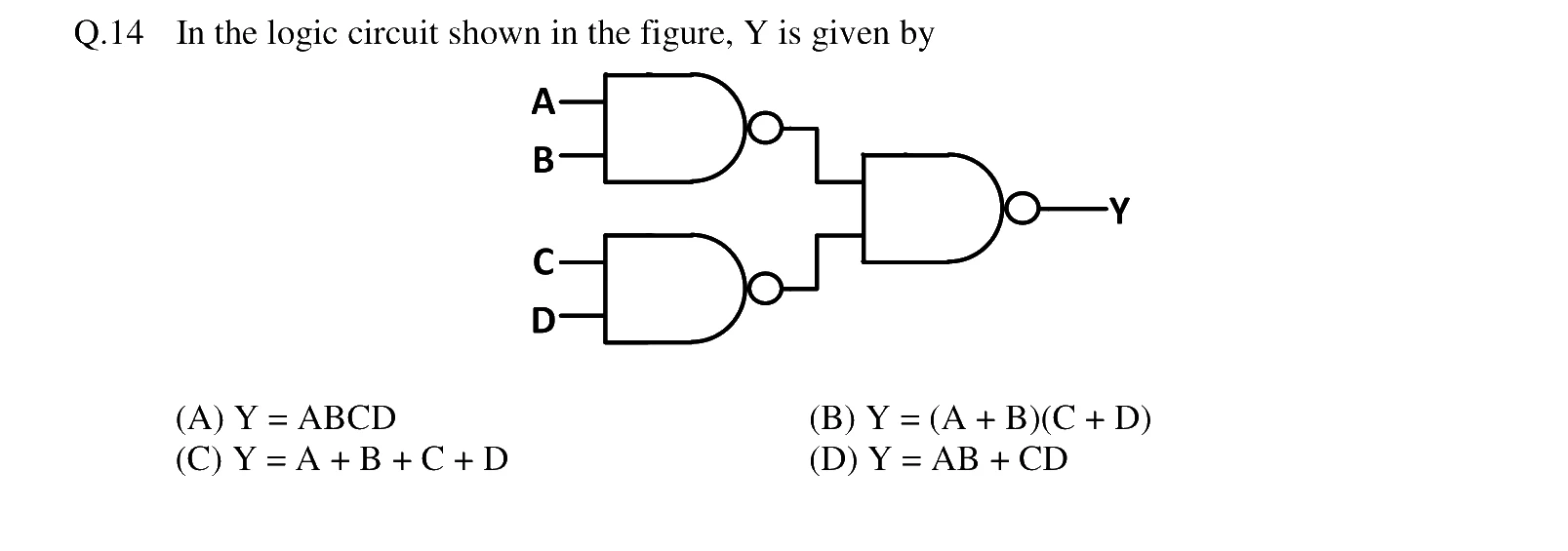
- 48EE 2018 · 1 mark · MCQ · ModerateThe op-amp shown in the figure is ideal. The input impedance is given by
- 49EE 2018 · 2 marks · MCQ · ModerateWhich one of the following statements is true about the digital circuit shown in the figure
- 50EE 2018 · 2 marks · MCQ · EasyDigital input signals with as the MSB and as the LSB are used to realize the Boolean function , where denotes the minterm. In addition, has a don't care for . The simplified expression for is given by
- 51EE 2018 · 2 marks · NAT · HardIn the circuit shown in the figure, the bipolar junction transistor (BJT) has a current gain . The base-emitter voltage drop is a constant, . The value of the Thevenin equivalent resistance (in ) as shown in the figure is ____ (up to 2 decimal places).
- 52EE 2017 Set 2 · 1 mark · MCQ · ModerateFor a 3-input logic circuit shown below, the output can be expressed as
- 53EE 2017 Set 2 · 2 marks · MCQ · ModerateFor the circuit shown in the figure below, it is given that . The transistor has and when the B-E junction is forward biased.
- 54EE 2017 Set 2 · 2 marks · MCQ · ModerateFor the circuit shown below, assume that the OPAMP is ideal.
- 55EE 2017 Set 2 · 2 marks · NAT · HardFor the synchronous sequential circuit shown below, the output is zero for the initial conditions .
- 56EE 2016 Set 2 · 1 mark · MCQ · ModerateThe output expression for the Karnaugh map shown below is
- 57EE 2016 Set 2 · 1 mark · MCQ · ModerateThe circuit shown below is an example of a
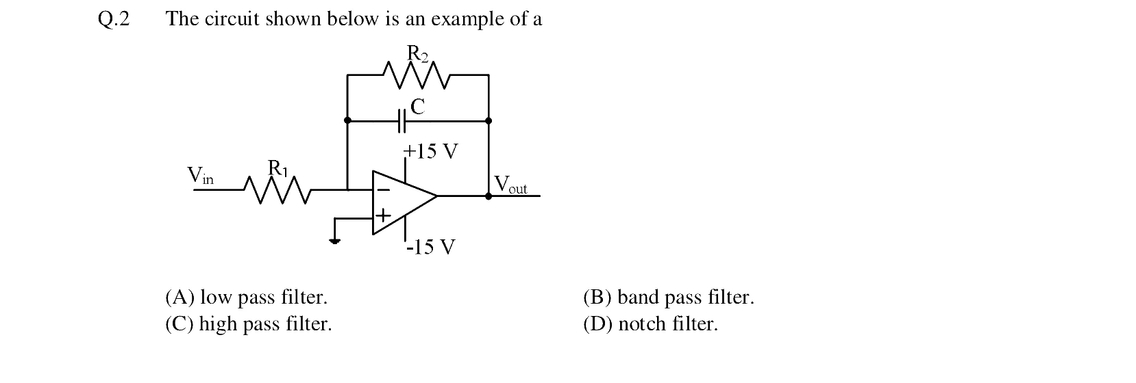
- 58EE 2016 Set 2 · 2 marks · MCQ · EasyThe Boolean expression simplifies to
- 59EE 2016 Set 2 · 2 marks · MCQ · ModerateFor the circuit shown below, taking the opamp as ideal, the output voltage in terms of the input voltages , and is