27 questions0 / 27 done
Questions per paper
- All
- MCQ
- MSQ
- NAT
2021 to 2026. Point at a year to read it.
Show as a table
| Year | All | MCQ | MSQ | NAT |
|---|---|---|---|---|
| 2021 | 0 | 0 | 0 | 0 |
| 2022 | 3 | 2 | 1 | 0 |
| 2023 | 5 | 4 | 0 | 1 |
| 2024 | 6 | 5 | 0 | 1 |
| 2025 | 8 | 4 | 3 | 1 |
| 2026 | 5 | 3 | 0 | 2 |
- 1EC 2026 · 1 mark · MCQ · ModerateThe ideal OP-AMP circuit shown in the Figure produces output voltage
- 2EC 2026 · 2 marks · MCQ · HardA small signal source, is applied to a BJT circuit as shown in the Figure.
- 3EC 2026 · 2 marks · MCQ · ModerateA circuit using an ideal OP-AMP is shown in the Figure.
- 4EC 2026 · 2 marks · NAT · ModerateConsider an ideal OP-AMP circuit as shown in the Figure.
- 5EC 2026 · 2 marks · NAT · ModerateConsider the ideal diodes D1 and D2 as shown in the Figure with cut-in voltage and is in .
- 6EC 2025 · 1 mark · MCQ · EasyA simplified small-signal equivalent circuit of a BJT-based amplifier is given below.
- 7EC 2025 · 1 mark · MCQ · ModerateThe ideal BJT in the circuit given below is biased in the active region with a of .
- 8EC 2025 · 1 mark · MSQ · EasyWhich of the following statements is/are TRUE with respect to an ideal opamp?
- 9EC 2025 · 1 mark · MSQ · ModerateWhich of the following statements is/are TRUE with respect to ideal MOSFET-based DC-coupled single-stage amplifiers having finite load resistors?
- 10EC 2025 · 1 mark · NAT · ModerateAll the components in the bandpass filter given below are ideal. The lower frequency of the filter is .
- 11EC 2025 · 2 marks · MCQ · ModerateThe identical MOSFETs and in the circuit given below are ideal and biased in the saturation region. and have a transconductance of .
- 12EC 2025 · 2 marks · MCQ · ModerateIn the circuit shown, the identical transistors Q1 and Q2 are biased in the active region with . The Zener diode is in the breakdown region with and .
- 13EC 2025 · 2 marks · MSQ · ModerateAll the diodes in the circuit given below are ideal.
- 14EC 2024 · 1 mark · MCQ · ModerateIn the circuit below, assume that the long channel NMOS transistor is biased in saturation. The small signal trans-conductance of the transistor is . Neglect body effect, channel length modulation and intrinsic device capacitances. The small signal input impedance is ____.
- 15EC 2024 · 1 mark · MCQ · ModerateFor the closed loop amplifier circuit shown below, the magnitude of open loop low frequency small signal voltage gain is 40. All the transistors are biased in saturation. The current source is ideal. Neglect body effect, channel length modulation and intrinsic device capacitances. The closed loop low frequency small signal voltage gain (rounded off to three decimal places) is ____.
- 16EC 2024 · 1 mark · NAT · ModerateAs shown in the circuit, the initial voltage across the capacitor is , with the switch being open. The switch is then closed at . The total energy dissipated in the ideal Zener diode () after the switch is closed (in mJ, rounded off to three decimal places) is __________.
- 17EC 2024 · 2 marks · MCQ · ModerateThe opamps in the circuit shown are ideal, but have saturation voltages of .
- 18EC 2024 · 2 marks · MCQ · ModerateIn the circuit below, the opamp is ideal.
- 19EC 2024 · 2 marks · MCQ · ModerateIn the circuit shown below, the transistors and are biased in saturation. Their small signal transconductances are and respectively. Neglect body effect, channel length modulation and intrinsic device capacitances.
- 20EC 2023 · 1 mark · MCQ · ModerateIn the circuit shown below, and are bias voltages. Based on input and output impedances, the circuit behaves as a
- 21EC 2023 · 1 mark · MCQ · EasyA cascade of common-source amplifiers in a unity gain feedback configuration oscillates when
- 22EC 2023 · 2 marks · MCQ · ModerateThe of the circuit shown below is
- 23EC 2023 · 2 marks · MCQ · ModerateIn the circuit shown below, and are silicon diodes with cut-in voltage of . and are input and output voltages in volts. The transfer characteristic is
- 24EC 2023 · 2 marks · NAT · ModerateIn the circuit below, the voltage is (rounded off to two decimal places).
- 25EC 2022 · 1 mark · MCQConsider the CMOS circuit shown in the figure (substrates are connected to their respective sources). The gate width () to gate length () ratios of the transistors are as shown. Both the transistors have the same gate oxide capacitance per unit area. For the , the threshold voltage is and the mobility of holes is . For the , the threshold voltage is and the mobility of electrons is . The steady state output voltage is _____.
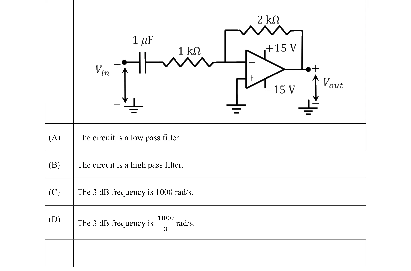
- 26EC 2022 · 1 mark · MSQAn ideal OPAMP circuit with a sinusoidal input is shown in the figure. The frequency is the frequency at which the magnitude of the voltage gain decreases by from the maximum value. Which of the options is/are correct?
- 27EC 2022 · 2 marks · MCQA circuit with an ideal OPAMP is shown. The Bode plot for the magnitude (in dB) of the gain transfer function () of the circuit is also provided (here, is the angular frequency in ). The values of and are _________.